
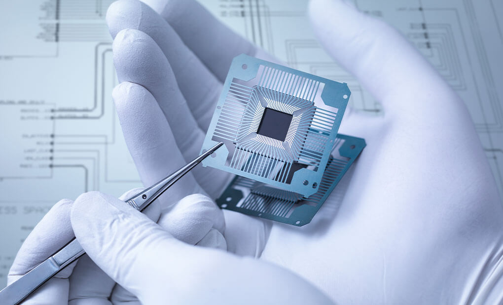
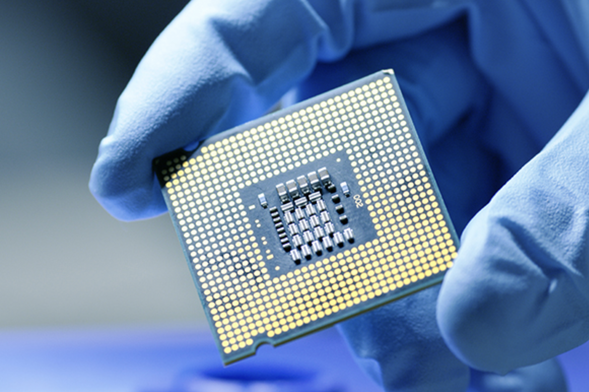
In the semiconductor industry, precision, reliability, and scalability define success. As electronic devices become smaller, faster, and more powerful, the demand for ultra-fine metal components with exacting tolerances continues to grow. Among these components, lead frames play a crucial role — they form the electrical connection between the semiconductor chip and the external circuitry of an integrated circuit (IC) package. To meet modern requirements for miniaturization and high performance, chemical etching has become one of the most advanced and efficient manufacturing methods for producing semiconductor lead frames.
The Role of Lead Frames in Semiconductor Packaging
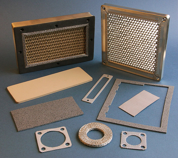
A lead frame serves as both a mechanical support and an electrical pathway. It anchors the semiconductor die in place, conducts signals between the chip and the printed circuit board (PCB), and helps dissipate heat generated during operation. Traditionally, lead frames were produced by stamping or photolithographic electroplating, but as device geometries have shrunk and multi-layer packaging technologies have evolved, these conventional methods have reached their technical limits.
For modern ICs — such as QFP (Quad Flat Package), QFN (Quad Flat No-lead), BGA (Ball Grid Array), and advanced system-in-package (SiP) designs — dimensional precision, edge definition, and material consistency are critical. Even microscopic defects or burrs can affect electrical performance and bonding reliability. This is where chemical etching stands out.
2. Precision Through Photochemical Etching
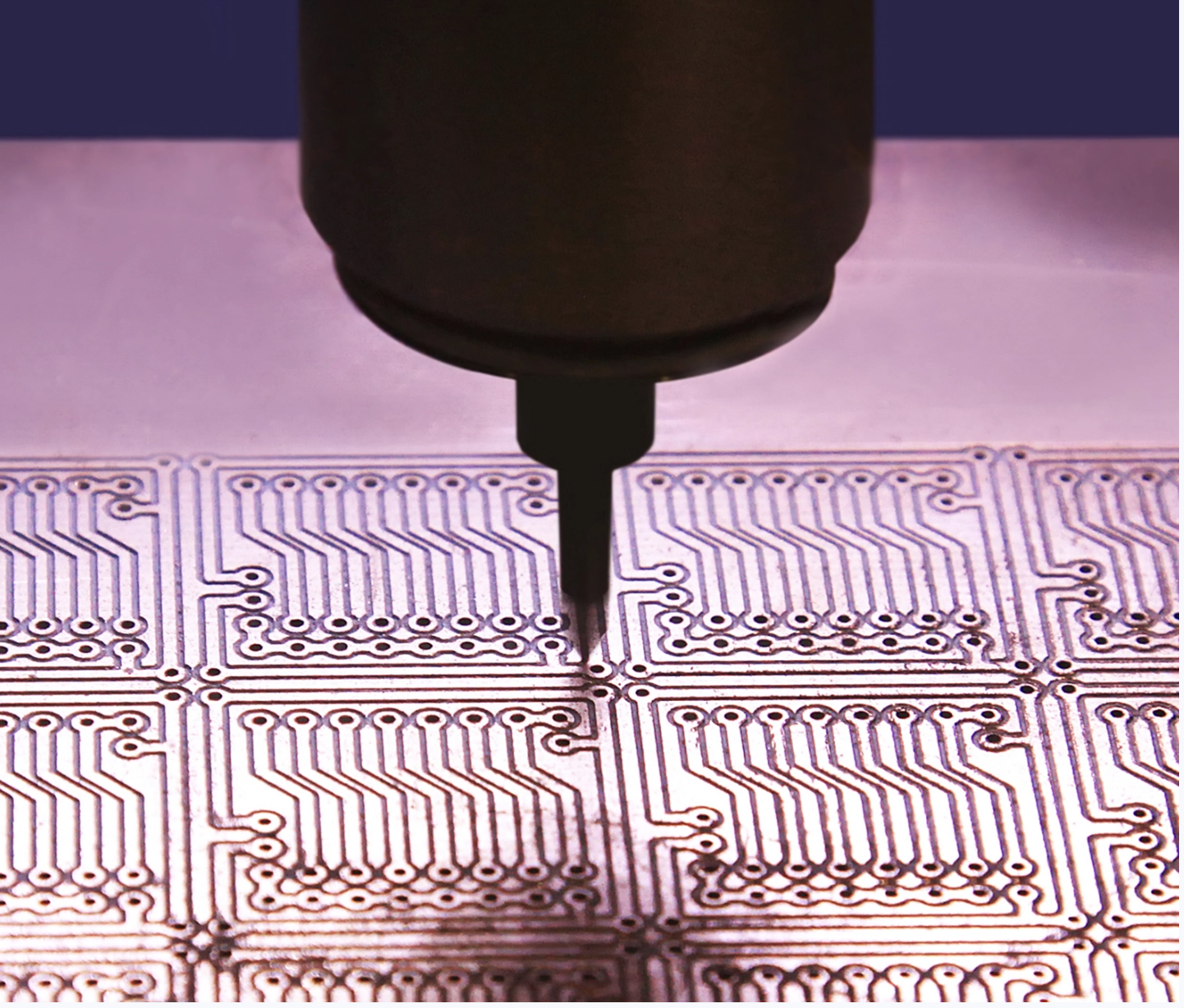
Chemical etching, also known as photochemical machining (PCM), uses a combination of photoresist imaging and chemical dissolution to selectively remove metal from thin sheets, typically made of copper, copper alloys, or other conductive materials. The process begins with cleaning and laminating the metal sheet with a light-sensitive photoresist film. The desired lead frame pattern is then transferred onto the surface through UV exposure and developed to reveal the areas to be etched.
When the sheet is immersed in an etching solution, the exposed regions are dissolved away with extraordinary precision, leaving behind the designed circuit pattern. Because the process is completely contact-free, there is no mechanical deformation, stress, or burr formation. Dimensional tolerances as fine as ±0.01 mm can be achieved, and the resulting edges are smooth and uniform — ideal for fine-pitch lead frame applications.
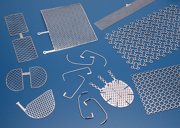
Another advantage of chemical etching is its ability to create complex geometries and micro-features that are impossible or uneconomical to produce by stamping. Fine leads, half-etched zones for selective thickness control, and intricate interconnect patterns can be formed on both sides of the metal simultaneously, supporting the most advanced semiconductor packaging designs.
3. Cost Efficiency and Rapid Prototyping
Unlike mechanical tooling, which requires expensive dies and long setup times, chemical etching relies on digital photo tooling, which can be prepared quickly and modified at minimal cost. This allows semiconductor manufacturers to move rapidly from prototype to production. Design iterations can be implemented within hours, enabling engineers to test multiple geometries or adjust dimensions according to packaging requirements without incurring large tooling expenses.
In mass production, chemical etching also offers scalability and cost stability. Hundreds of identical lead frames can be produced from a single sheet in one batch, ensuring high throughput and consistent quality. Since there is no tool wear or deformation, repeatability remains extremely high throughout production, resulting in fewer defects and lower scrap rates.
4. Material and Surface Integrity
For semiconductor lead frames, maintaining the integrity of the metal is essential for ensuring long-term reliability and high electrical conductivity. Chemical etching removes material at the molecular level without applying force or heat, preserving the original mechanical and electrical properties of the base metal. This contrasts sharply with stamping or laser cutting, which may introduce microcracks, stress, or thermal damage that can weaken the final product.
The etching process also provides superior surface quality. The edges are clean and burr-free, reducing the risk of short circuits or bonding failures during chip assembly. The smooth surface ensures excellent adhesion for subsequent plating processes such as silver, nickel-palladium-gold, or tin finishes — all commonly applied to improve solderability and corrosion resistance.
5. Flexibility Across Designs and Materials
One of the defining advantages of chemical etching is design flexibility. Whether producing ultra-thin fine-pitch QFN frames or multi-layer stackable structures for high-density packaging, the process can be adapted to various materials and thicknesses. Copper, Alloy 42 (Fe-Ni alloy), and stainless steel are commonly etched with equal precision, supporting diverse electrical and thermal performance needs.
Moreover, chemical etching allows for dual-sided patterning, where different depths or shapes can be etched on each surface. This capability enables the production of special functional features such as half-etched bonding areas, selective tie bars, and integrated ground planes — features that are difficult or impossible to achieve with traditional mechanical fabrication.
6. Sustainability and Clean Manufacturing
Modern chemical etching processes have also evolved to meet global environmental standards. State-of-the-art etching lines incorporate advanced filtration, waste recovery, and chemical recycling systems to minimize environmental impact. Since the process is clean, quiet, and energy-efficient, it contributes to the sustainability goals of semiconductor manufacturers aiming for greener production lines.
7. Conclusion
In an era where the semiconductor industry demands ever-smaller, more efficient, and more complex devices, chemical etching has proven to be an indispensable technology. It provides the precision, flexibility, and scalability necessary to manufacture next-generation lead frames with micron-level accuracy and defect-free surfaces. By combining cost-effectiveness, rapid prototyping capability, and material integrity, chemical etching not only meets today’s challenges but also prepares manufacturers for the future of semiconductor innovation.
As semiconductor packaging continues to evolve — from traditional ICs to advanced 3D integration and chiplet architectures — chemical etching will remain at the heart of this transformation, enabling the connection between technology and precision at the microscopic scale.
Chemical Etching Technology in Semiconductor Lead Frame Manufacturing
In the semiconductor industry, precision, reliability, and scalability define success. As electronic devices become smaller, faster, and more powerful, the demand for ultra-fine metal components with exacting tolerances continues to grow. Among these components, lead frames play a crucial role — they form the electrical connection between the semiconductor chip and the external circuitry of an integrated circuit (IC) package. To meet modern requirements for miniaturization and high performance, chemical etching has become one of the most advanced and efficient manufacturing methods for producing semiconductor lead frames.
1. The Role of Lead Frames in Semiconductor Packaging
A lead frame serves as both a mechanical support and an electrical pathway. It anchors the semiconductor die in place, conducts signals between the chip and the printed circuit board (PCB), and helps dissipate heat generated during operation. Traditionally, lead frames were produced by stamping or photolithographic electroplating, but as device geometries have shrunk and multi-layer packaging technologies have evolved, these conventional methods have reached their technical limits.
For modern ICs — such as QFP (Quad Flat Package), QFN (Quad Flat No-lead), BGA (Ball Grid Array), and advanced system-in-package (SiP) designs — dimensional precision, edge definition, and material consistency are critical. Even microscopic defects or burrs can affect electrical performance and bonding reliability. This is where chemical etching stands out.